03 Research Projects
Blood Pressure Sensor
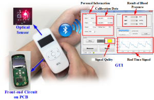
This program is designed to design a front-end analog circuit for a non-invasive, piezoresistive blood pressure sensing array with easy access to the data. The circuit has an automatic correction function. This is a self-correcting system for a sensor array designed for optimal array of pulse blood pressure sensor arrays, which is aligned with the signal between the sensors in the array sensor, corrected in the interpolation mode, Signal variation, so that subjects do not have to worry about the location of each time the problem of accurate. So far has been completed pulse signal sensing and signal processing, fruitful. Has established a front-end analog read circuit and digital analog converter, which front analog read circuit operation mode is through the Wheatstone bridge sensor resistance sensor deformation of the resistance changes, the output of the corresponding voltage signal, and a The amplifier will be the signal for the amplification action; and then analog signal into a digital signal before the need to use a low-pass filter out the signal contained in the high-frequency noise components to avoid the case of Aliasing (Aliasing) And finally connected to a successor analogue digital converter (Successive approximation ADC) analog signal will be converted into digital signals. The resulting wafer is optimized for measurement and performance, and the printed circuit design and planning of the printed circuit are completed. The wireless transmission circuit will further use the Bluetooth transmission and will be integrated into the sensor to optimize the design results in the form of system chips (SoC) chip off the assembly line. Through the program designed by the system of the chip, the Bluetooth transmission mode to send the signal to the subprogram four to establish the cloud database for blood pressure and vascular compression deformation of the alignment and correction, transmission to the computer, mobile phones and other devices to obtain immediate blood pressure, in order to facilitate observation and monitoring.
The so-called “proximity sensing device” is a non-contact type sensing device that does not touch to detect the proximity of the object. Can be divided into capacitive proximity sensor, inductive proximity sensor, Hall effect proximity sensor and light sensor. As for the light proximity sensing device we use the light source for the polymer light-emitting diode (PLED), this device is organic light-emitting diodes and organic light sensor (Photodiode) component characteristics of the application, by organic light two The polar body generates an optical signal that is reflected by the measured object and is received by the organic photodetector to determine the movement of the object by detecting the intensity of the photocurrent.
In particular, the use of (PLED) organic components to produce light proximity sensor, can reduce the production costs, and to achieve the characteristics of flexibility. Mainly for the light detector to receive objects reflected back to the optical signal, designed to active pixel sensing mode read circuit, the so-called active pixels are no need for external circuit with the direct read circuit and sensing device integrated layout On a single wafer.”
Touch-type display panel applications more and more common, the current touch panel in the rest of the world has begun to become an industry, with advanced equipment, it is the simplest and convenient multimedia information equipment, touch panel with many advantages such as ruggedness and space saving. At present, this laboratory is focused on the design of capacitive touch panel and back-end sensing IC design, the theoretical and simulation software to calculate the capacitance value and a variety of situations, and then with the simulation of the capacitance value of the IC design.”
03 Research Projects
Readout Circuits
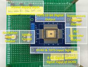
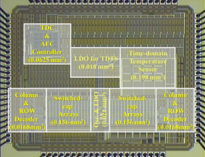
This topic presents a 16-MHz digital-controlled crystal oscillator and a time-domain temperature sensor design to achieve a high-precision auto calibration temperature-compensated crystal oscillator in a low-power mobile device. The digital-controlled crystal oscillator is based on Pierce readout topology with two 8-bit switched-capacitor arrays. The temperature is measured with the temperature-dependent delays of the proposed delay cell, called time-domain temperature sensor. The supply voltage of digital-controlled crystal oscillator and time-domain temperature sensor are regulated at 1.2 V by using two on-chip low-dropout regulators. The designed circuit has been successfully fabricated by using TSMC 0.18-μm CMOS process, where the active area is 2.2 mm2. The measured phase noise of 1 kHz offset at 25C is -116.37 dB/Hz. The frequency deviation over -40˚C to 85˚C is within +/- 0.2 ppm after compensation. The measured effective temperature resolution of the time-domain temperature sensor is 0.18˚C/LSB and the measured error is within -2˚C to 1.6˚C at 1k Hz conversion rate. The measured current consumption of the chip is about 2.5 mA.
Keywords: Crystal oscillator, Digital control, Temperature compensation, Low power, Delay cell, Temperature sensor.
The design for the design of mobile speaker algorithm and circuit implementation, the period can be maintained in the acceptable linear performance range, and not Affect the speaker lifetime situation, adjust the drive current to reach the speaker the best way to drive.
Very low powerdisplay Suitable for use in battery devices such as electronic watches, computers, sphygmomanometers, weight gauges, blood glucose gauges (Glucometer) , Smart Meter Card, Oxygen Concentrator, Pulse Oximeter, Continuous Positive Pressure Respirator, (ECAK), low-power display, as long as the black and white color is enough, and the mainstream display has a completely different direction of development The At first glance, sales of a wide variety of products is difficult to reduce costs. But STN did, STN applications, although the number of sales and a wide variety, but the STN LCD specifications are not so much, compared to its display and driver IC has a large sales and limited market characteristics of the mainstream. The new generation of low-power display is the electrophoretic display (Electro-Phoretic Display, EPD), commonly known as electronic paper (e-paper), has been able to do red, black and white colors (E-Ink Spectra). Applied in the smart glasses products Google Glass LCoS micro-projection display technology, allowing users to get like a large-size screen visual enjoyment.
This study is designed to use a bipolar high voltage for LCD panels to develop a DC-to-DC converter that uses a conventional PWM control Boost boost circuit. The boost circuit designed in this study can convert a single input voltage to four bipolar voltage output levels (± 12V and ± 6V) with only a single external inductor, and can be solved by a dynamic charge algorithm The advantages of the traditional PWM control, the characteristics of this boost circuit can be operated in asymmetric load conditions, fast transient response and light load conditions can still maintain high conversion efficiency , this study has been through the CIC chip off the assembly line and Verification, can effectively reduce the cost of LCD panel production and size.
In recent years, the market for portable sensors has grown rapidly, with micro-sized gas sensors, whether in general indoor air detection, Measuring and so play a very important role, the potential market is also gradually improved. However, the most important issue for portable products is how to reduce power to facilitate the use of batteries for long-term detection, how to balance low power, accuracy and read speed is an important task.
The purpose of this project is to design ultra-thin folding capacitive touch screen display panel and its ultra-thin Type noise compensation sensing circuit. In the past for capacitive touch panel design to take more than the value of mutual capacitance, and then measure the touch before and after the change, ultra-thin folding capacitive touch panel inparticular when the Hard coat thinning may change the finger touch on the The extent of the impact of the electrode, may cause changes in capacitance from the mutual capacitance changes, resulting in multi-touch when the accuracy of the problem, in view of this, we must simulate the ultra-thin touch panel in the touch when the capacitor phenomenon And build the model. The compensation sensing method is designed by simulation results. In addition, complete the detection of finger touch on the back-end driver verification platform.
Electromagnetic hunting interface circuit and its system IC design of the spindle by the design of a new type of electromagnetic hunting device can be placed in any vibration source such as the human body can generate electricity, analyze its power generation and equivalent circuit Modeland to This design-interface circuit recovers the electrical energy generated by this mechanism, and finally integrates the circuit into the IC , and combines the PCB circuit board design and the use of SMD components to miniaturize it to become an independent integrated power generation system device Can extend battery life and life, or can be used in micro-energy electronic circuit device can be maintained for a long time operation without additional charge or replace the battery.
In the 103- year plan, we aimed at the infrared gas sensor (IC) , the infrared gas sensor, the infrared gas sensor, the infrared gas sensor, the infrared gas sensor, the infrared gas sensor, the infrared gas sensor, Design, refer to other literature, and use software simulation to design the best infrared gas sensor. The design of this gas sensing system, we hope that this sensor can be installed into the phone, with real-time detection, easy to carry advantage, can really give the sensor in the environmental testing and the value brought about.
The goal of this project is to use a liquid crystal optical element of a Liquid Crystal Lens Array, which is based on the concept of Lenticular Lens Sheet in 3D display technology, based on the 2.8” panel (CPT Small Application 2.8”), And to achieve 2-view type for the purpose. In order to increase the effective distance between the user and the display of the original 3D display can be freely adjusted by the user, the project uses a new liquid crystal optical element (novel electrode design) LC Lens Sheet, replacing the original 3D display technology optical elements – Lenticular Lens Sheet application. Not only retain the advantages of the original Lenticular Lens Sheet , and because of LC Lens for the voltage- adjustable liquid crystal optical components , so according to the size of the voltage applied to the free adjustment of the display and the viewer’s 3D viewing distance; LC Lens Sheet A flat structure, unlike LG ‘s LC Lens for 3D displays, is a semi-circular electrode structure, and then it needs to be integrated into the display panel, and the process is greatly reduced.
Mainly based on liquid crystal technology and the development of the variable zoom liquid crystal lens (Liquid Crystal Lens) components. This lens effectively utilizes the optical properties of the liquid crystal to make it have great potential for development. The electric field is controlled by the external voltage. The polarization direction of the photoelectric field is different from that of the liquid crystal molecule. The refractive index is also different. Into a similar GRIN Lens optical components, the advantage is that you can use the external electric field to control the focal length of the optical components, unlike the traditional optical lens for the fixed focal length. The most important part of the liquid crystal lens is to try to produce a refractive index difference, so that the refractive index for the gradient distribution, so that the light can focus or divergence. The structure of this liquid crystal lens is similar to the principle of liquid crystal screen, for two conductive glass (ITO) filled between the liquid crystal, and then use the electric field to control the refractive index of liquid crystal, and by the refractive index distribution (Gradient refractive index) to achieve the focus Function, while controlling the focal length, to make convex lens effect.
This study focuses on the design of microelectromechanical (MEMS) capacitive microphones before the read circuit, due to portable low voltage operation of the electronic products increasingly robust, therefore, will focus on mobile applications microelectromechanical (MEMS) condenser microphone in the low Voltage low power operation under the preamplifier. Micro-electromechanical condenser microphones contain two main circuits, one for the center-point self-bias capacitor-to- voltage converter circuit, and the other for the amplifier. Among them, the amplifier is related to the characteristics of the signal in this paper, the beginning of the design of the general second-order operational amplifier, although the amplifier can smoothly amplify the signal, at a fixed magnification, the different input swing, and frequency. Corresponding to the ideal magnification under the signal is different. Thus, the design of the second class op amp has a non-linear magnification and a lower output swing. So, then switch to symmetrical rail-to-rail operational amplifiers to improve the linearity and output swing of the circuit. The circuit of this study is based on Taiwan’s 0.35um (2P4M, 3.3V / 5V) process to complete the wafer production process. The output voltage range is approximately in the range of positive and negative voltage sources, and the total circuit power consumption is about 200uW. In addition to the design of low-pass filter and high-pass filter, thereby reducing the high-frequency noise and filter out the input DC bias.
03 Research Projects
AMOLED Driver Circuit
With the development of scientific and technological progress, TFT LCD has completely replaced the traditional display technology. Organic light-emitting diodes (OLEDs) are considered to be thefuture of the TFT LCD, the future of the most development potential of the flat display technology. The principle of light emission is the potential difference between the electrons injected into the electrons and the holes due to the applied voltage so that these electron holes are moved in the film layer and the recombination is generated. This recombination energy will High energy and non-stable excitation state, when the light energy is released when it will return to the low energy and stable ground state, resulting in the so-called injection-type electroluminescence. It has the advantages of active light emission, high response speed characteristics, power saving, light and so on, and the other process is simple and low cost, can be applied to the characteristics of flexible panels, known as one of the most ideal display, but still can not put a lot of Production, the main reason is that the panel can not improve the uniformity and deterioration of components and other issues, the study will address the above issues and add the rest of the method to improve the method.
With the development of scientific and technological progress, TFT LCD has completely replaced the traditional display technology. Organic light-emitting diodes (OLEDs) are considered to be thefuture of the TFT LCD, the future of the most development potential of the flat display technology. The principle of light emission is the potential difference between the electrons injected into the electrons and the holes due to the applied voltage so that these electron holes are moved in the film layer and the recombination is generated. This recombination energy will High energy and non-stable excitation state, when the light energy is released when it will return to the low energy and stable ground state, resulting in the so-called injection-type electroluminescence. It has the advantages of active light emission, high response speed characteristics, power saving, light and so on, and the other process is simple and low cost, can be applied to the characteristics of flexible panels, known as one of the most ideal display, but still can not put a lot of Production, the main reason is that the panel can not improve the uniformity and deterioration of components and other issues, the study will address the above issues and add the rest of the method to improve the method.
03 Research Projects
Energy Harvesting
The program focuses on the development of miniature energy harvesting accumulators used in automotive wireless tire pressure detection systems (TPMS). Working principle for the energy acquisition, conversion process power control technology. Will be based on the micro-hunting device energy generation range and output changes to do a specific discussion, due to the acquisition of energy is very small situation, the boost converter or regulator power loss should be minimized, so the power conversion Circuit research, we will first use the input energy storage circuit analysis and design to build low-loss conversion circuit, followed by this small hunting device energy conversion characteristics of the development of dynamic adaptive control strategy for the above do circuit matching research, and put forward Efficient switching circuit architecture and a wide range of voltage range control strategies in a variety of operating modes, while the circuit management in the system energy transfer to reduce the application of circuit power loss, to achieve the maximum efficiency of energy collection as the goal. Expect the next plan to design the IC chip with the relevant concepts to miniaturize the circuit and reduce energy consumption.”
Solar energy is currently available for development and utilization of green alternative energy in a more potential for development. The development of solar energy is mainly based on photoelectric conversion, and the research is committed to improving the solar energy materials to enhance its photocurrent, by virtue of this purpose to enhance the efficiency of solar power generation system. However, regardless of how the performance of solar cell materials to enhance, its biggest drawback is the power generation efficiency by the impact of sunshine intensity, and since the beginning are not effective to improve the results. Therefore, the laboratory solar energy conversion circuit, is designed a storage circuit in the shade, cloudy, rainy days can still continue to store energy, so that the back-end Inverter circuit to normal action, in order to enhance the overall efficiency of solar energy.”