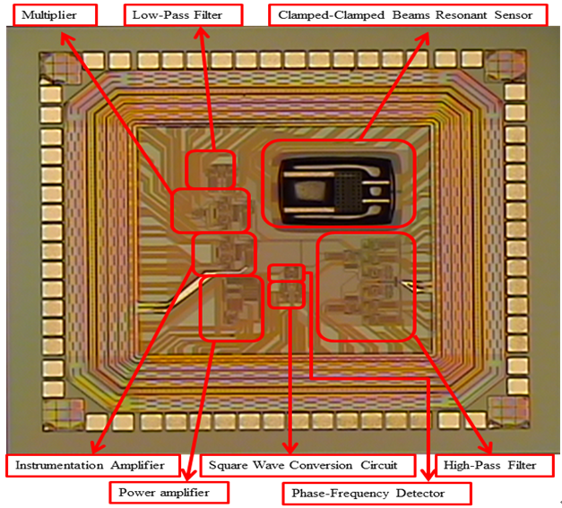
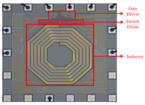
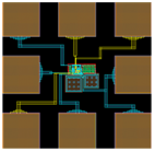
This study presents a novel gas sensor in the form of a micro-machined resonator and its readout circuit. The resonator has the structure of clamped-clamped beams with thermal actuation and piezo-resistive sensing that supports a plate capable of being attached with test gas molecules to detect gas concentration. The purpose of this study was to design a new gas sensor readout system for a clamped-clamped beam resonator with thermal actuation and piezo-resistive sensing and also presents a new approach to reject the feed-through noise. The readout circuits and micro-machined resonant gas sensor are realized on a single chip. The sensor is driven by a DDS module and power amplifier, and then sense the vibrations by piezo-resistivity. The piezo-resistivity is detected by a Wheatstone bridge circuits. The carried signal of modulation is set in Wheatstone bridge circuits. An instrumentation amplifier adjusts the gain to the appropriate amplitude. The circuit with reduction on feed-through noise increases the SNR. Square wave conversion circuit and PFD process the signal and the driver reference signal to detect phase difference. The data of phase difference is counted into a microcontroller dsPIC4011 and then the data being transmitted to the computer by RS232 to a USB adapter. Finally, the circuit and the micro-machined resonator are fabricated by Taiwan Semiconductor Manufacturing Company (TSMC) 0.35μm 2P4M 3.3V.mixed‐signal CMOS process and one-step post-processing. The proposed chips, in a die area of 1.847×1.847 mm2, are carried out with the help of National Chip Implementation Center (CIC).
A new output buffer amplifier with digital analog conversion reduces the cost and power consumption of the source driver of a liquid crystal display. The principle of the buffer amplifier with two input voltage level, by controlling the input differential pair of the tail current size, change the two input side of the weight relationship, making the buffer amplifier linear interpolation of an output voltage between the two input voltage. In this way, by controlling the differential current of the tail current to produce digital analog conversion circuit function, reduce the resistance string digital analog converter order, to save the area of the function. In the text, the concept and principle of circuit design, as well as the experimental results are fully introduced and explained. The circuit proposed in this paper is simulated and implemented using the TSMC 0.35mm 2P4M process, which is an output buffer amplifier with a 10-bit analog-to-digital converter, with an output buffer settling time of 2.5msec with a tens of bit analog The converter’s output buffer amplifier area is 0.0095mm2, requiring only 38% of the traditional octet resistance string digital analog converter area.
A new optical image stabilizer (OIS) for mobile phone cameras is proposed. The whole study is completed step by step, the optimization of the magnetic field, the dynamic analysis and the realization of the controller. The past optical image stabilizer uses a two-dimensional plane displacement mechanism, but this design of the compensation effect is more limited, the design of the use of dual-axis rotation mechanism to compensate, this body by the voice coil motor (VCM) to control the rotation angle , To take pictures when the anti-shake effect. (2) the establishment of the dynamic model of the system and the derivation of the dynamic equation; (3) the smooth mode (2) the establishment of the dynamic model of the system; (3) the smooth mode ( SMC) controller design and implementation. The first part uses the CAD software to carry out the mechanism design, the establishment of this optical shadow stabilizer of the biaxial (pitch axis and yaw axis) rotation mechanism, which includes the camera lens module suspension device, magnet and coil composed of small voice coil motor Actuators and so on, and in order to reduce the volume and remove the yoke yoke (yoke), and then through the genetic algorithm to optimize the design of magnetic circuit, to obtain a stable and suitable magnetic field. The second part is devoted to the dynamic analysis of this biaxial rotation system and the dynamic equation (EOM) derivation. According to the method proposed by Lagrange, the dynamic equation of the whole optical image stabilizer can be generated by deducing the kinetic energy and compensating current The relationship between the electromagnetic moment to derive, whereby the equation can be designed corresponding to the controller. After the completion of the foregoing work, the third part focuses on the application of smooth mode control theory and the construction of the controller. First, after simulating and experimenting to verify the effectiveness of the controller, the system is built by the actual circuit. Test of anti-shake function of the product.
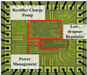
An electromagnetic hunt mechanism is proposed to convert the vibrational energy in the environment into electromagnetic energy by means of electromagnetic induction. The design of a self-adjusting non-voltage drop charging pump and the rear power management circuit and regulator The interface circuit collects the tiny alternating energy generated by the microreactor and converts it into DC energy for use by the electronic device or directly supplies power to the microsystems. In order to make the collection of energy more efficient, this paper also proposed dedicated to this rectifier charging pump optimization method. In this paper, the proposed micro-hunting circuit, the peak can be greater than 0.7 volts of AC energy, converted to 3.3 volts DC power; In addition, the self-adjusting pressure-free charge pump can be based on our proposed optimization Method, automatically adjust the charge pump when the output of the hunting device changes the order of the system conversion efficiency to maintain high efficiency, and its non-pressure drop of the rectifier characteristics also reduce the energy consumption during the consumption, power management circuit can be based on monitoring Load device and hunting device output power status of the energy transfer for effective control. With the optimization method proposed in this paper, the energy extracted by the charge pump is 1.3% error relative to the maximum energy, while the transition to the transition capacitance is only 1.63%. The paper proposed in this paper, are successful by TSMC 0.35 micron process simulation and implementation.
Organic light-emitting diodes have many advantages, such as high contrast, high reaction speed, self-luminous, high viewing angle, low power consumption, etc., is regarded as one of the next generation of potential flat panel display. However, the main reason why it has not yet been able to produce mass production is that the panel uniformity can not be improved and the life expectancy of component deterioration. The problem of panel uniformity is mainly driven by long-term driving of thin film transistor (TFT) in Pixel The problem of component life will be caused by varying degrees of drift; component deterioration of the life problem is driven by constant current density driven, the components of the internal light-emitting layer of electrons and holes continue to accumulate, making the effect of recombination luminescence deterioration, resulting in component degradation, and thus make the brightness decreased. In this paper, a current mirror structure to compensate for the drift of the characteristics of the TFT, the design to pulse width modulation (PWM) principle to reduce the current density to improve the component degradation effect, while the OLED component without current through, to negative bias The active organic light emitting diode pixel circuit which compensates the uniformity of the panel and improves the deterioration of the element luminous efficiency in the luminous layer on the OLED element. In addition to the traditional current-driven pixel circuit of the current source is not easy to create shortcomings, to create a relatively simple voltage-driven type, in order to reduce the complexity of circuit production. In this paper, the LTPS TFT Model Card is used as the simulation reference to verify the designed circuit characteristics. Finally, the QVGA panel is manufactured by AUO’s LTPS SPC process and the deterioration measurement is carried out to verify the improvement of the component degradation.
For lithium batteries due to rapid charge caused by the rapid rise in temperature to compensate for the situation, and with the completion of photovoltaic systems with immediate temperature rise suppression of lithium battery fast charging system. The most important research of the photovoltaic system is to capture the maximum power of the current solar array to give the back-end load, that is, the maximum power tracking, which is different from the traditional maximum power tracking technology. In this paper, the fuzzy control is used to complete the intelligent solar maximum power tracking controller , This controller can quickly and accurately track the maximum power point. With the front-end solar power generation, this paper designed three DC-DC converter circuit to adjust the system power supply back-end load, the conversion circuit for the two-step boost converter circuit, step-down conversion circuit and flyback conversion circuit. Design a step-down conversion circuit, with the design of the charging law — constant current charging, pulse charging, small current charge and discharge. The fuzzy controller completes the maximum power tracking of the solar energy in the constant current charging and pulse charging mode to charge the current when the maximum power is supplied, and adjusts the output current of the solar array in the micro current charging and discharging mode to achieve the setting of the minute current. Pulse charging law is based on the battery temperature feedback to control the charge cycle of its charge and then to achieve the effect of suppressing the rapid rise in battery temperature, and small current charging is the purpose of charging the battery charge to 100% SOC (State of Charge). In this paper, the proposed method of fast charging with battery temperature rise suppression can effectively utilize the PV system to achieve fast and safe charging target.
The proposed novel gas reading circuit is designed specifically for organic vertical nanometer junction diode gas sensors, which utilizes this design circuit to integrate the front end gas sensor into a gas sensing system. The read system consists of seven parts, the first part of which is a preamplifier, which consists of a transimpedance amplifier for the purpose of converting the output current of the gas sensor into a voltage change. The sixth part is a logic gate and a buffer. When the sensor is reacting with the gas and the reaction is saturated, the result is output through the logic gate and the buffer. Otherwise, it is displayed as zero. The seventh part is the microprocessor, using the ALIENTEK STM32, the central processor for the ARM Cortex ™ -M, we use one of the analog digital converters for analog conversion circuit output conversion, and then LCD display results The This circuit utilizes TSMC 0.35μm 2P4M 3.3V mixed-signal complementary gold-oxygen semiconductor process to design a specially designed circuit from the IC. The wafer was designed to be 1.083 × 1.04 mm2, 1.082 × 1.082 mm2 and 0.74 × 0.75 mm2, respectively, under the terms of the wafer design by the National Experimental Institute of the Chip System Design Center. The system combined with the front-end sensor for analog gas sensor output current measurement, has actually tested its feasibility. Different from the traditional instrument of the measurement environment, the gas sensing system design, with real-time detection, easy to carry, low cost and reduce the advantages of human error, can really give health care sensor in the home medical aspects of the value.
This study will be based on the liquid crystal display driver system (Liquid crystal display Driver System) by the battery system to provide a stable 2.8 volts to 5 volts boost function, although the inductive DC boost circuit has been quite mature and sufficient research, But the inductor for the portable consumer products to pursue the goal of minimizing the purpose of the volume is accounted for too large a volume ratio, and contains the total inductance of the chip inductive DC boost circuit related research is very rare, so the The study mainly discusses the inductive DC booster circuit, which is distributed together with the inductor in the CMOS chip, and optimizes the influence of the inductance, frequency and the circuit of each component, and adjusts the control of the inductive DC boost circuit (TSIC) is commissioned by the National Chip Research Center (CIC) at the National Chip Research Center (CIC), which is based on the geometrical model of the geometrical model of the printed circuit board and the minimum inductance of the printed circuit board under the specific inductance and resistance values. To 0.35um process to achieve the design circuit, and then measure the overall circuit performance, with the traditional discrete inductance group The DC boost circuit inductor merits do volume, efficiency and practicality of the comparison.
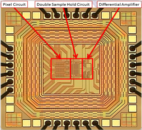
(Active Pixel Sensor (APS)), and the “three-dimensional optical proximity sensor read circuit” combined with active pixel circuit and background light subtraction circuit to achieve the function of sensing close objects The The objective of the three-dimensional optical proximity sensing system is to develop a set of non-contact touch panels that not only have all the flat (two-dimensional) sensing of the touch panel on the market, but also increase the sensitivity of the third axis height, And enhance the “three-dimensional” proximity sensor, do not touch the panel to be able to sense the location of the object. The front panel is composed of a light emitting diode (LED) and an optical receiver. The light emitting diode emits light to the object to be detected and receives the reflected light from the optical receiver. The object is judged by the intensity of the reflected light distance. In order to apply to different environments and background light, you need to do a special design of the circuit to do the background light to eliminate the action, and finally through the program to write algorithms and man-machine interface, calculate the coordinates of the object to be measured. The active pixel circuit is often used in complementary gold-oxygen semiconductor light sensor (CMOS SENSOR), as a light receiver (Photo Detector, PD) drive circuit, the main role is to detect the light sensor (3T-APS), the drawback of this circuit is that the output swing of this circuit is limited, and the output of the circuit is limited by the fact that the light intensity is converted to a voltage value and there is an advantage of increasing the resolution and reducing the alien noise. , The maximum value can not reach the upper limit of the bias. In this paper, a new active pixel circuit is proposed, which can extend the output swing to the upper limit of the bias voltage, thus increasing the resolution of the active pixel, whether it is used in the complementary gold-oxygen semiconductor light sensor or the optical Proximity sensing circuit, will be better than the previous 3T architecture output performance. Circuit successfully off the line to TSMC 0.35um2P4M 3.3V mixed signal complementary gold-oxygen semiconductor process, the specially designed circuit from the IC to achieve, combined with the front panel and back-end program to form the entire system, has actually tested its feasibility. The wafer was sponsored by the Chip System Design Center of the National Experimental Institute of the Foundation, with two wafer areas of 1.289 x 1.289 mm2 and 0.8 x 1.220 mm2, respectively.
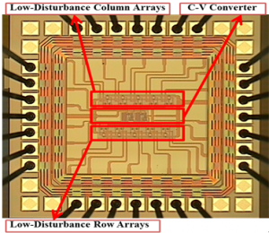
Capacitive touch screen is made of indium tin oxide (ITO) transparent conductive film, due to contact with the panel after the ITO electrode capacitance between the size of the change in the size of the object to determine the situation. Large-size capacitive touch panel is unique in that the resistance of ITO is very large (> 200KΩ), will make the tiny capacitance of the signal attenuation, it is difficult to determine whether the fingers touch, and large-size capacitive touch In addition to the large value of the panel, but also by the surrounding temperature, humidity … and other environmental interference factors, making the panel measured ITO capacitance is not fixed, with the surrounding environment changes. In the past, the capacitive touch circuit design to take more DC way to charge and discharge the capacitor, and then measure the touch before and after the change, this method can be applied to small size panel, because of its ITO caused by the smaller resistance (10KΩ ). The large-size capacitive touch panel front-end sensing circuit proposed in this paper is designed for 12-inch or more projection capacitive touch panel, and can be used to detect the panel capacitance in the form of AC, which can greatly reduce the DC drive Of the capacitor charge and discharge time. The two sensing circuits proposed in this paper are the integrator sensing circuit and the differential comparison sensing circuit. The two circuits are matched with the low-interference scanning array at the front end. The array can reduce the environment on the ITO And the touch panel of the front-end of the circuit is measured by the 12.1-inch projected capacitive touch panel provided by Qiling Technology. In the integrator sensing circuit section, the low interference scanning array and the capacitance-voltage conversion circuit are formed, and the part of the differential comparison circuit is composed of a low interference scanning array, a capacitive bridge circuit and a differential amplifier circuit, Off the line into IC for measurement. Finally, by the FPGA to write UART transmission chip and VB program language to the computer serial data transmission, and send the value to the computer analysis. The sensing circuit part of this paper has been successfully off the assembly line to TSMC 0.35um 2P4M 3.3V mixed signal complementary gold-oxygen semiconductor process, combined with the front 12.1-inch capacitive touch panel and back-end program to form the entire system, and has the actual Test its feasibility. The research on the underside chip was sponsored by the Chip System Design Center of the National Experimental Institute, 1.281 × 1.281 mm2 and 0.91 × 0.775 mm2, respectively.
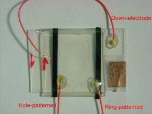
In addition to using the voltage to change the focal length, and the design of a new type of upper electrode design, including the ring and multi-layer and add a set of external voltage regulation, a substantial improvement in LCD lens due to increased aperture caused by refractive index as the perfect focus of the refractive index Distribution, whereby the new lens improves the focus quality to facilitate modularization with mobile phones or other imaging systems. As the traditional basic liquid crystal lens effective focusing aperture to more than 2 mm in diameter will be due to the refractive index distribution, such as trapezoidal, resulting in the central part of the flat area can not focus, only the edge part of the focus. This new type of liquid crystal lens design Another set of external electrodes to improve the distribution of non-uniform electric field As we expected, this electrode is based on the refractive index of the refractive index of the lens design, the use of 2DMOS simulation software simulation of electric field and refractive index distribution, Length and verify the effect of changing the focal length. And the physical measurement and verification of the new liquid crystal lens focal length changes and optical focus quality.
This study is mainly designed for microelectromechanical (MEMS) capacitive microphones before the read circuit, due to portable low voltage operation of electronic products increasingly robust, therefore, will focus on mobile applications microelectromechanical (MEMS) condenser microphone in the low Voltage low power operation under the preamplifier. Micro-electromechanical condenser microphones contain two main circuits, one for the center-point self-bias capacitor-to-voltage converter circuit, and the other for the amplifier. Among them, the amplifier is related to the characteristics of the signal in this paper, the beginning of the design of the general second-order operational amplifier, although the amplifier can smoothly amplify the signal, but at a fixed magnification, the different input swing and frequency, Corresponding to the ideal magnification under the signal is different. Thus, the design of the second class op amp has a non-linear magnification and a lower output swing. So, then switch to symmetrical rail-to-rail operational amplifiers to improve the linearity and output swing of the circuit. The circuit of this study is based on Taiwan’s 0.35um (2P4M, 3.3V / 5V) process to complete the wafer production process. The output voltage range is approximately in the range of positive and negative voltage sources, and the total circuit power consumption is about 200uW. In addition to the design of low-pass filter and high-pass filter, thereby reducing the high-frequency noise and filter out the input DC bias.